To compensate for an offset voltage by injecting a current you can apply an adjustable voltage from a potentiometer via a high-value resistor to an appropriate circuit node. To adjust a “ground” voltage that a resistor connects to, you can connect it to a potentiometer which is able to vary either side of ground.
Q. Why offset nulling is used in op amp?
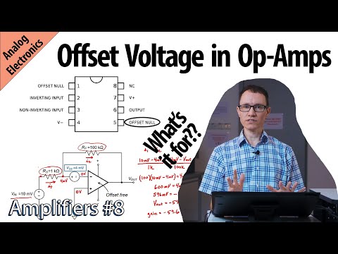
Implementing offset null within the op amp The op amp offset null circuitry adds a balance capability to the input circuitry as shown in the example of the 741 op amp input stage. The op amp offset null connections enable the input circuit balance to be obtained by applying external circuitry.
Table of Contents
- Q. Why offset nulling is used in op amp?
- Q. What is offset voltage in op amp?
- Q. What is offset adjustment?
- Q. How is offset voltage calculated?
- Q. How do you adjust offset null?
- Q. Which factor is responsible for causing slew rate?
- Q. How can I increase my CMRR value?
- Q. What is common mode gain?
- Q. What is the advantage of using an active load?
- Q. Which circuit is used as active load for an amplifier?
- Q. How the performance of an op amp circuit can be improved?
- Q. What happens when the operating frequency of an op-amp increase?
- Q. Which factor makes the differentiator circuit unstable?
- Q. What is gain limiting frequency?
- Q. What happens if the input frequency is kept lower than the frequency at which the gain is zero?
- Q. What is the effect of gain on bandwidth?
- Q. How can I increase the bandwidth of my amplifier?
- Q. What is the significance of gain bandwidth product?
Q. What is offset voltage in op amp?
The input offset voltage is defined as the voltage that must be applied between the two input terminals of the op amp to obtain zero volts at the output. Ideally the output of the op amp should be at zero volts when the inputs are grounded.
Q. What is offset adjustment?
If one thing is offset by another, the effect of the first thing is reduced by the second, so that any advantage or disadvantage is cancelled out. verb (=balance) The increase in pay costs was more than offset by higher productivity… be V-ed.
Q. How is offset voltage calculated?
The circuit amplifies the input offset voltage by the noise gain of 1001. The measurement is made at the amplifier output using an accurate digital voltmeter. The offset referred to the input (RTI) is calculated by dividing the output voltage by the noise gain.
Q. How do you adjust offset null?
To make the voltages exactly equal, you apply the same voltage to both pins and place a potentiometer to one of the pins and change the resistance until the output is 0V. Offset null adjustment requires a potentiometer with its wiper connected to the negative supply (with some op amps) or to 0V (with others).
Q. Which factor is responsible for causing slew rate?
Which factor is responsible for causing slew rate? Explanation: Capacitors require a finite amount of time to charge and discharge. Thus, a capacitor inside or outside the op-amp causes slew rate.
Q. How can I increase my CMRR value?
Besides supplying constant emitter current, the constant current bias also provides a very high source resistance since the ac equivalent or the dc source is ideally an open circuit. viii. High resistance RE will reduce the common mode gain thus improving the CMRR.
Q. What is common mode gain?
Common-mode voltage gain refers to the amplification given to signals that appear on both inputs relative to the common (typically ground). You will recall from a previous discussion that a differential amplifier is designed to amplify the difference between the two voltages applied to its inputs.
Q. What is the advantage of using an active load?
It turns out that an additional (and perhaps somewhat unexpected) benefit of active loading is that it converts the output signal from differential to single-ended without loss of gain.
Q. Which circuit is used as active load for an amplifier?
current mirror circuit
Q. How the performance of an op amp circuit can be improved?
How the performance of an op-amp circuit can be improved? Explanation: The compensating networks are used to improve /modify the performance of an op-amp circuit over the desired frequency range by controlling it gain and phase shift.
Q. What happens when the operating frequency of an op-amp increase?
What happens when the operating frequency of an op-amp increase? Explanation: When the operating frequency is increased the gain of the amplifier decrease. As it is linearly related to frequency, the phase shift is logarithmically related to frequency.
Q. Which factor makes the differentiator circuit unstable?
which factor makes the differentiator circuit unstable? Explanation: The gain of the differentiator circuit (RF / XC1) increases with increase in frequency at a rate of 20dB/decade. This makes the circuit unstable.
Q. What is gain limiting frequency?
The gain limiting frequency is given by. The circuit acts as an integrator in the frequency range fa to fb. the value of fa and in turn R1CF and RFCF values should be selected such. that fab. Thus the output is proportional to the time integral of the input.
Q. What happens if the input frequency is kept lower than the frequency at which the gain is zero?
What happens if the input frequency is kept lower than the frequency at which the gain is zero? Explanation: If the input frequency is lower that the lower frequency limit of the integrator (i.e. when gain = 0), there will be no integration results and the circuit act like a simple inverting amplifier.
Q. What is the effect of gain on bandwidth?
The op amp gain bandwidth product is constant for voltage-feedback amplifiers. However it is not applicable for current feedback amplifiers because relationship between gain and bandwidth is not linear. Therefore decreasing the gain by a factor of ten will increase the bandwidth by the same factor.
Q. How can I increase the bandwidth of my amplifier?
Bandwidth of an amplifier may be increased by lowering the lower cut-off frequency and/or increasing the upper cut-off frequency.
Q. What is the significance of gain bandwidth product?
Relevance to design. This quantity is commonly specified for operational amplifiers, and allows circuit designers to determine the maximum gain that can be extracted from the device for a given frequency (or bandwidth) and vice versa.